
Organic electronics

Organic electronicsis a field ofmaterials scienceconcerning the design,synthesis,characterization, and application oforganicmolecules orpolymersthat show desirableelectronicproperties such asconductivity.Unlike conventional inorganicconductorsandsemiconductors,organic electronic materials are constructed from organic (carbon-based) molecules or polymers using synthetic strategies developed in the context oforganic chemistryandpolymer chemistry.
One of the promised benefits of organic electronics is their potential low cost compared to traditional electronics.[1][2][3]Attractive properties of polymeric conductors include their electrical conductivity (which can be varied by the concentrations ofdopants) and comparatively high mechanicalflexibility.Challenges to the implementation of organic electronic materials are their inferiorthermal stability,high cost, and diverse fabrication issues.
History[edit]
- Electrically conductive polymers
Traditional conductive materials areinorganic,especiallymetalssuch ascopperandaluminumas well as manyalloys.[citation needed]
In 1862Henry Lethebydescribedpolyaniline,which was subsequently shown to be electrically conductive. Work on other polymeric organic materials began in earnest in the 1960s. For example in 1963, a derivative of tetraiodopyrrole was shown to exhibit conductivity of 1 S/cm (S =Siemens).[4]In 1977, it was discovered that oxidation enhanced the conductivity ofpolyacetylene.The 2000 Nobel Prize in Chemistry was awarded toAlan J. Heeger,Alan G. MacDiarmid,andHideki Shirakawajointly for their work on polyacetylene and related conductive polymers.[5]Many families of electrically conducting polymers have been identified includingpolythiophene,polyphenylene sulfide,and others.
J.E. Lilienfeld[6]first proposed thefield-effect transistorin 1930, but the first OFET was not reported until 1987, when Koezuka et al. constructed one usingPolythiophene[7]which shows extremely high conductivity. Otherconductive polymershave been shown to act as semiconductors, and newly synthesized and characterized compounds are reported weekly in prominent research journals. Many review articles exist documenting the development of thesematerials.[8][9][10][11][12]
In 1987, the first organicdiodewas produced atEastman KodakbyChing W. TangandSteven Van Slyke.[13]
- Electrically conductive charge transfer salts
In the 1950s, organic molecules were shown to exhibit electrical conductivity. Specifically, the organic compoundpyrenewas shown to form semiconducting charge-transfer complexsaltswithhalogens.[14]In 1972, researchers found metallic conductivity (conductivity comparable to a metal) in the charge-transfer complexTTF-TCNQ.
- Light and electrical conductivity
André Bernanose[15][16]was the first person to observeelectroluminescencein organicmaterials.Ching W. Tang andSteven Van Slyke,[17]reported fabrication of the first practical OLED device in 1987. The OLED device incorporated a double-layer structure motif composed ofcopper phthalocyanineand a derivative ofperylenetetracarboxylic dianhydride.[18]
In 1990, apolymerlight emitting diodes was demonstrated byBradley,Burroughes,Friend.Moving from molecular to macromolecular materials solved the problems previously encountered with the long-term stability of the organic films and enabled high-quality films to be easily made.[19]In the late 1990's, highly efficient electroluminescent dopants were shown to dramatically increase the light-emitting efficiency of OLEDs[20]These results suggested that electroluminescent materials could displace traditional hot-filament lighting. Subsequent research developed multilayer polymers and the new field of plastic electronics andorganic light-emitting diodes(OLED) research and device production grew rapidly.[21]
Conductive organic materials[edit]

Organic conductive materials can be grouped into two main classes: polymers and conductivemolecularsolids and salts.Polycyclic aromaticcompounds such aspentaceneandrubreneoften form semiconducting materials when partially oxidized.
Conductive polymersare often typically intrinsically conductive or at least semiconductors. They sometimes show mechanical properties comparable to those of conventional organic polymers. Bothorganicsynthesis and advanceddispersiontechniques can be used to tune theelectricalproperties ofconductive polymers,unlike typicalinorganicconductors. Well-studied class ofconductive polymersincludepolyacetylene,polypyrrole,polythiophenes,andpolyaniline.Poly(p-phenylene vinylene) and itsderivativesareelectroluminescentsemiconducting polymers. Poly(3-alkythiophenes) have been incorporated into prototypes ofsolar cellsandtransistors.
Organic light-emitting diode[edit]
An OLED (organic light-emitting diode) consists of a thin film of organic material that emits light under stimulation by an electric current. A typical OLED consists of an anode, a cathode, OLED organic material and a conductive layer.[23]


OLED organicmaterialscan be divided into two major families: small-molecule-based and polymer-based. Small molecule OLEDs (SM-OLEDs) includetris(8-hydroxyquinolinato)aluminium[17]fluorescentandphosphorescentdyes, and conjugateddendrimers.Fluorescentdyescan be selected according to the desired range ofemissionwavelengths;compounds likeperyleneandrubreneare often used. Devices based on small molecules are usually fabricated bythermalevaporationundervacuum.While this method enables the formation of well-controlled homogeneousfilm;is hampered by high cost and limited scalability.[24] [25]Polymer light-emitting diodes (PLEDs) are generally more efficient than SM-OLEDs. Common polymers used in PLEDs includederivativesof poly(p-phenylene vinylene)[26]andpolyfluorene.The emittedcolorby the structure of the polymer. Compared to thermal evaporation,solution-based methods are more suited to creatingfilmswith large dimensions.
Organic field-effect transistor[edit]

An organic field-effect transistor (OFET) is a field-effect transistor utilizing organic molecules or polymers as the active semiconducting layer. A field-effect transistor (FET) is any semiconductor material that utilizeselectric fieldto control the shape of a channel of one type ofchargecarrier, thereby changing its conductivity. Two major classes ofFETare n-type and p-type semiconductor, classified according to the charge type carried. In the case of organic FETs (OFETs), p-type OFET compounds are generally more stable than n-type due to the susceptibility of the latter to oxidative damage.
As for OLEDs, some OFETs are molecular and some are polymer-based system.Rubrene-based OFETs show high carrier mobility of 20–40 cm2/(V·s). Another popular OFET material isPentacene.Due to its lowsolubilityin most organicsolvents,it's difficult to fabricate thin film transistors (TFTs) from pentacene itself using conventional spin-cast or,dip coatingmethods, but this obstacle can be overcome by using the derivative TIPS-pentacene.
Organic electronic devices[edit]

Organic solar cellscould cut the cost of solar power compared with conventional solar-cell manufacturing.[27]Siliconthin-film solar cellson flexible substrates allow a significant cost reduction of large-area photovoltaics for several reasons:[28]
- The so-called 'roll-to-roll'-deposition on flexible sheets is much easier to realize in terms of technological effort than deposition on fragile and heavyglass sheets.
- Transport and installation of lightweight flexible solar cells also saves cost as compared to cells on glass.
Inexpensive polymeric substrates likepolyethylene terephthalate(PET) orpolycarbonate(PC) have the potential for further cost reduction in photovoltaics.Protomorphoussolar cells prove to be a promising concept for efficient and low-cost photovoltaics on cheap and flexible substrates for large-area production as well as small and mobile applications.[28]
One advantage of printed electronics is that different electrical and electronic components can be printed on top of each other, saving space and increasing reliability and sometimes they are all transparent. One ink must not damage another, and low temperature annealing is vital if low-cost flexible materials such as paper andplastic filmare to be used. There is much sophisticated engineering and chemistry involved here, with iTi, Pixdro, Asahi Kasei, Merck & Co.|Merck, BASF, HC Starck, Hitachi Chemical and Frontier Carbon Corporation among the leaders.[29] Electronic devicesbased onorganic compoundsare now widely used, with many new products under development.Sonyreported the first full-color, video-rate, flexible, plastic display made purely of organicmaterials;[30][31]televisionscreen based on OLED materials;biodegradableelectronics based on organic compound and low-cost organicsolar cellare also available.
Fabrication methods[edit]
Small molecule semiconductors are ofteninsoluble,necessitatingdepositionvia vacuumsublimation.Devices based onconductive polymerscan be prepared by solution processing methods. Both solution processing and vacuum based methods produce amorphous andpolycrystallinefilms with variable degree of disorder. "Wet"coatingtechniques require polymers to be dissolved in a volatilesolvent,filtered and deposited onto asubstrate.Common examples of solvent-based coating techniques include drop casting,spin-coating,doctor-blading,inkjet printingandscreen printing.Spin-coating is a widely used technique for small areathin filmproduction. It may result in a high degree of material loss. The doctor-blade technique results in a minimal material loss and was primarily developed for large area thin film production. Vacuum based thermal deposition of small molecules requiresevaporationof molecules from a hot source. The molecules are then transported through vacuum onto a substrate. The process of condensing these molecules on the substrate surface results in thin film formation. Wet coating techniques can in some cases be applied to small molecules depending on their solubility.
Organic solar cells[edit]
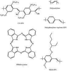
Organic semiconductor diodes convert light into electricity. Figure to the right shows five commonly used organic photovoltaic materials. Electrons in these organic molecules can be delocalized in a delocalized πorbitalwith a corresponding π* antibondingorbital.The difference in energy between the π orbital, or highest occupied molecular orbital (HOMO), and π* orbital, or lowest unoccupied molecular orbital (LUMO) is called theband gapof organic photovoltaic materials. Typically, theband gaplies in the range of 1-4eV.[32][33][34]
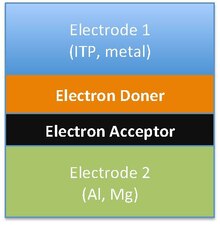
The difference in theband gapof organicphotovoltaicmaterials leads to different chemical structures and forms of organicsolar cells.Different forms of solar cells includes single-layer organicphotovoltaiccells, bilayer organicphotovoltaiccells and heterojunctionphotovoltaiccells. However, all three of these types of solar cells share the approach of sandwiching the organic electronic layer between two metallic conductors, typicallyindium tin oxide.[35]

Organic field-effect transistors[edit]
An organic field-effect transistor is a three terminal device (source, drain and gate). The charge carriers move between source and drain, and the gate serves to control the path's conductivity. There are mainly two types of organic field-effect transistor, based on the semiconducting layer's charge transport, namely p-type (such as dinaphtho[2,3-b:2′,3′-f]thieno[3,2-b]thiophene, DNTT),[36]and n-type (such phenyl C61 butyric acid methyl ester, PCBM).[37]Certain organic semiconductors can also present both p-type and n-type (i.e., ambipolar) characteristics.[38]
Such technology allows for the fabrication of large-area, flexible, low-cost electronics.[39]One of the main advantages is that being mainly a low temperature process compared to CMOS, different type of materials can be utilized. This makes them in turn great candidates for sensing.[40]
Features[edit]
Conductive polymersare lighter, moreflexible,and less expensive than inorganic conductors. This makes them a desirable alternative in many applications. It also creates the possibility of new applications that would be impossible using copper or silicon.
Organic electronics not only includesorganic semiconductors,but also organicdielectrics,conductors andlight emitters.
New applications includesmart windowsandelectronic paper.Conductive polymersare expected to play an important role in the emerging science ofmolecular computers.
See also[edit]
References[edit]
- ^Hagen Klauk (Ed.)Organic Electronics: Materials, Manufacturing and Applications2006, Wiley-VCH, Weinheim. PrintISBN9783527312641.
- ^Hagen Klauk (Ed.)Organic electronics. More materials and applications2010, Wiley-VCH, Weinheim.ISBN9783527640218electronic bk.
- ^Paolo Samori, Franco CacialliFunctional Supramolecular Architectures: for Organic Electronics and Nanotechnology2010 WileyISBN978-3-527-32611-2
- ^McNeill, R.; Siudak, R.; Wardlaw, J. H.; Weiss, D. E. (1963). "Electronic Conduction in Polymers. I. The Chemical Structure of Polypyrrole".Aust. J. Chem.16(6): 1056–1075.doi:10.1071/CH9631056.
- ^"The Nobel Prize in Chemistry 2000".Nobelprize.org. Nobel Media.
- ^CA 272437,Lilienfeld, Julius Edgar, "Electric current control mechanism", published 1927-07-19
- ^Koezuka, H.; Tsumura, A.; Ando, T. (1987). "Field-effect transistor with polythiophene thin film".Synthetic Metals.18(1–3): 699–704.doi:10.1016/0379-6779(87)90964-7.
- ^Hasegawa, Tatsuo; Takeya, Jun (2009)."Organic field-effect transistors using single crystals".Sci. Technol. Adv. Mater.(free download).10(2): 024314.Bibcode:2009STAdM..10b4314H.doi:10.1088/1468-6996/10/2/024314.PMC5090444.PMID27877287.
- ^Yamashita, Yoshiro (2009)."Organic semiconductors for organic field-effect transistors".Sci. Technol. Adv. Mater.(free download).10(2): 024313.Bibcode:2009STAdM..10b4313Y.doi:10.1088/1468-6996/10/2/024313.PMC5090443.PMID27877286.
- ^Dimitrakopoulos, C.D.; Malenfant, P.R.L. (2002)."Organic Thin Film Transistors for Large Area Electronics".Adv. Mater.14(2): 99.doi:10.1002/1521-4095(20020116)14:2<99::AID-ADMA99>3.0.CO;2-9.
- ^Reese, Colin; Roberts, Mark; Ling, Mang-Mang; Bao, Zhenan (2004)."Organic thin film transistors".Mater. Today.7(9): 20.doi:10.1016/S1369-7021(04)00398-0.
- ^Klauk, Hagen (2010). "Organic thin-film transistors".Chem. Soc. Rev.39(7): 2643–66.doi:10.1039/B909902F.PMID20396828.
- ^Forrest, S. (2012)."Energy efficiency with organic electronics: Ching W. Tang revisits his days at Kodak".MRS Bulletin.37(6): 552–553.Bibcode:2012MRSBu..37..552F.doi:10.1557/mrs.2012.125.
- ^Mulliken, Robert S. (January 1950)."Structures of Complexes Formed by Halogen Molecules with Aromatic and with Oxygenated Solvents 1".Journal of the American Chemical Society.72(1): 600–608.doi:10.1021/ja01157a151.ISSN0002-7863.
- ^Bernanose, A.; Comte, M.; Vouaux, P. (1953). "A new method of light emission by certain organic compounds".J. Chim. Phys.50:64–68.doi:10.1051/jcp/1953500064.
- ^Bernanose, A.; Vouaux, P. (1953). "Organic electroluminescence type of emission".J. Chim. Phys.50:261–263.doi:10.1051/jcp/1953500261.
- ^abTang, C. W.; Vanslyke, S. A. (1987). "Organic electroluminescent diodes".Applied Physics Letters.51(12): 913.Bibcode:1987ApPhL..51..913T.doi:10.1063/1.98799.
- ^Forrest, Stephen R. (2020)."Waiting for Act 2: What lies beyond organic light-emitting diode (OLED) displays for organic electronics?".Nanophotonics.10(1): 31–40.Bibcode:2020Nanop..10..322F.doi:10.1515/nanoph-2020-0322.
- ^Burroughes, J. H.; Bradley, D. D. C.; Brown, A. R.; Marks, R. N.; MacKay, K.; Friend, R. H.; Burns, P. L.; Holmes, A. B. (1990)."Light-emitting diodes based on conjugated polymers".Nature.347(6293): 539–541.Bibcode:1990Natur.347..539B.doi:10.1038/347539a0.S2CID43158308.
- ^Baldo, M. A.; O'Brien, D. F.; You, Y.; Shoustikov, A.; Sibley, S.; Thompson, M. E.; Forrest, S. R. (1998). "Highly efficient phosphorescent emission from organic electroluminescent devices".Nature.395(6698): 151–154.Bibcode:1998Natur.395..151B.doi:10.1038/25954.S2CID4393960.
- ^National Research Council (2015).The Flexible Electronics Opportunity.The National Academies Press. pp. 105–6.ISBN978-0-309-30591-4.
- ^D. Chasseau; G. Comberton; J. Gaultier; C. Hauw (1978). "Réexamen de la structure du complexe hexaméthylène-tétrathiafulvalène-tétracyanoquinodiméthane".Acta Crystallographica Section B.34(2): 689.doi:10.1107/S0567740878003830.
- ^Daniel J. Gaspar, Evgueni Polikarpov, ed. (2015).OLED Fundamentals: Materials, Devices, and Processing of Organic Light-Emitting Diodes(1 ed.). CRC Press.ISBN978-1466515185.
- ^Piromreun, Pongpun; Oh, Hwansool; Shen, Yulong; Malliaras, George G.; Scott, J. Campbell; Brock, Phil J. (2000). "Role of CsF on electron injection into a conjugated polymer".Applied Physics Letters.77(15): 2403.Bibcode:2000ApPhL..77.2403P.doi:10.1063/1.1317547.
- ^Holmes, Russell; Erickson, N.; Lüssem, Björn; Leo, Karl (27 August 2010). "Highly efficient, single-layer organic light-emitting devices based on a graded-composition emissive layer".Applied Physics Letters.97(1): 083308.Bibcode:2010ApPhL..97a3308S.doi:10.1063/1.3460285.
- ^Burroughes, J. H.; Bradley, D. D. C.; Brown, A. R.; Marks, R. N.; MacKay, K.; Friend, R. H.; Burns, P. L.; Holmes, A. B. (1990). "Light-emitting diodes based on conjugated polymers".Nature.347(6293): 539.Bibcode:1990Natur.347..539B.doi:10.1038/347539a0.S2CID43158308.
- ^Bullis, Kevin (17 October 2008)."Mass Production of Plastic Solar Cells".Technology Review.
- ^abKoch, Christian (2002)Niedertemperaturabscheidung von Dünnschicht-Silicium für Solarzellen auf Kunststofffolien,Doctoral Thesis, ipe.uni-stuttgart.de
- ^Raghu Das, IDTechEx (25 September 2008)."Printed electronics, is it a niche? – 25 September 2008".Electronics Weekly.Retrieved14 February2010.
- ^プラスチックフィルム thượng の hữu cơ TFT駆 động hữu cơ ELディスプレイで thế giới sơ の フルカラー tỏ vẻ を thật hiện.sony.co.jp (in Japanese)
- ^Flexible, full-color OLED display.pinktentacle (24 June 2007).
- ^Nelson J. (2002). "Organic photovoltaic films".Current Opinion in Solid State and Materials Science.6(1): 87–95.Bibcode:2002COSSM...6...87N.doi:10.1016/S1359-0286(02)00006-2.
- ^Halls J.J.M. & Friend R.H. (2001). Archer M.D. & Hill R.D. (eds.).Clean electricity from photovoltaics.London: Imperial College Press. pp. 377–445.ISBN978-1860941610.
- ^Hoppe, H.;Sarıçiftçi, N. S.(2004). "Organic solar cells: An overview".J. Mater. Res.19(7): 1924–1945.Bibcode:2004JMatR..19.1924H.doi:10.1557/JMR.2004.0252.
- ^McGehee D.G. & Topinka M.A. (2006). "Solar cells: Pictures from the blended zone".Nature Materials.5(9): 675–676.Bibcode:2006NatMa...5..675M.doi:10.1038/nmat1723.PMID16946723.S2CID43074502.
- ^Sugiyama, Masahiro; Jancke, Sophie; Uemura, Takafumi; Kondo, Masaya; Inoue, Yumi; Namba, Naoko; Araki, Teppei; Fukushima, Takanori; Sekitani, Tsuyoshi (September 2021)."Mobility enhancement of DNTT and BTBT derivative organic thin-film transistors by triptycene molecule modification".Organic Electronics.96:106219.doi:10.1016/j.orgel.2021.106219.
- ^Anthony, John E.; Facchetti, Antonio; Heeney, Martin; Marder, Seth R.; Zhan, Xiaowei (8 September 2010)."n-Type Organic Semiconductors in Organic Electronics".Advanced Materials.22(34): 3876–3892.doi:10.1002/adma.200903628.PMID20715063.S2CID205235378.
- ^Zhao, Yan; Guo, Yunlong; Liu, Yunqi (11 October 2013)."25th Anniversary Article: Recent Advances in n-Type and Ambipolar Organic Field-Effect Transistors".Advanced Materials.25(38): 5372–5391.doi:10.1002/adma.201302315.PMID24038388.S2CID6042903.
- ^Di, Chong-an; Zhang, Fengjiao; Zhu, Daoben (18 January 2013)."Multi-Functional Integration of Organic Field-Effect Transistors (OFETs): Advances and Perspectives".Advanced Materials.25(3): 313–330.doi:10.1002/adma.201201502.PMID22865814.S2CID26645918.
- ^Dudhe, Ravishankar S.; Sinha, Jasmine; Kumar, Anil; Rao, V. Ramgopal (30 June 2010)."Polymer composite-based OFET sensor with improved sensitivity towards nitro based explosive vapors".Sensors and Actuators B: Chemical.148(1): 158–165.doi:10.1016/j.snb.2010.04.022.ISSN0925-4005.
Further reading[edit]
- Grasser, Tibor., Meller, Gregor. Baldo, Marc. (Eds.) (2010)Organic electronicsSpringer, Heidelberg.ISBN978-3-642-04537-0(Print) 978-3-642-04538-7 (Online)
- Baracus, B. A.; Weiss, D. E. (1963). "Electronic Conduction in Polymers. II. The Electrochemical Reduction of Polypyrrole at Controlled Potential".Aust. J. Chem.16(6): 1076–1089.doi:10.1071/CH9631076.
- Bolto, B. A.; McNeill, R.; Weiss, D. E. (1963). "Electronic Conduction in Polymers. III. Electronic Properties of Polypyrrole".Aust. J. Chem.16(6): 1090–1103.doi:10.1071/CH9631090.
- Hush, Noel S. (2003). "An Overview of the First Half-Century of Molecular Electronics".Ann. N.Y. Acad. Sci.1006(1): 1–20.Bibcode:2003NYASA1006....1H.doi:10.1196/annals.1292.016.PMID14976006.S2CID24968273.
- Electronic Processes in Organic Crystals and Polymers, 2 ed.by Martin Pope and Charles E. Swenberg, Oxford University Press (1999),ISBN0-19-512963-6
- Handbook of Organic Electronics and Photonics(3-Volume Set) by Hari Singh Nalwa, American Scientific Publishers. (2008),ISBN1-58883-095-0
External links[edit]
 Media related toOrganic electronicsat Wikimedia Commons
- orgworld–Organic Semiconductor Worldhomepage.