
Zen 2
| General information | |
|---|---|
| Launched | 7 July 2019[1] |
| Designed by | AMD |
| Common manufacturers |
|
| CPUIDcode | Family 17h |
| Cache | |
| L1cache | 64 KB per core:
|
| L2 cache | 512 KB per core |
| L3 cache | 16 MB perCCX(APU: 8 MB) |
| Architecture and classification | |
| Technology node | TSMCN7[2][3] TSMCN6[4] |
| Instruction set | AMD64(x86-64) |
| Physical specifications | |
| Transistors |
|
| Cores |
|
| Sockets | |
| Products, models, variants | |
| Product code names |
|
| Brand names | |
| History | |
| Predecessor | Zen+ |
| Successor | Zen 3 |
| Support status | |
| Supported | |
Zen 2is acomputer processormicroarchitecturebyAMD.It is the successor ofAMD'sZenandZen+microarchitectures, and is fabricated on the7 nmMOSFETnode fromTSMC.The microarchitecture powers the third generation ofRyzenprocessors, known asRyzen 3000for the mainstream desktop chips (codename "Matisse" ),Ryzen 4000U/H(codename "Renoir" ) andRyzen 5000U(codename "Lucienne" ) for mobile applications, asThreadripper 3000for high-end desktop systems,[6][7]and asRyzen 4000Gforaccelerated processing units(APUs). The Ryzen 3000 series CPUs were released on 7 July 2019,[8][9]while the Zen 2-basedEpycserver CPUs (codename "Rome" ) were released on 7 August 2019.[10]An additional chip, the Ryzen 9 3950X, was released in November 2019.[8]
At CES 2019, AMD showed a Ryzen third-generationengineering samplethat contained one chiplet with eight cores and 16 threads.[6]AMD CEOLisa Sualso said to expect more than eight cores in the final lineup.[11]AtComputex2019, AMD revealed that the Zen 2 "Matisse" processors would feature up to 12 cores, and a few weeks later a 16 core processor was also revealed atE32019, being the aforementioned Ryzen 9 3950X.[12][13]
Zen 2 includes hardware mitigations to theSpectre security vulnerability.[14]Zen 2-based EPYC server CPUs use a design in which multiple CPU dies (up to eight in total) manufactured on a 7 nm process ( "chiplets") are combined with a 14nmI/Odie (as opposed to the 12nm IOD on Matisse variants) on each multi-chip module (MCM) package. Using this, up to 64 physical cores and 128 total compute threads (withsimultaneous multithreading) are supported per socket. This architecture is nearly identical to the layout of the "pro-consumer" flagship processor Threadripper 3990X.[15]Zen 2 delivers about 15% moreinstructions per clockthan Zen and Zen+,[16][17]the 14- and 12-nm microarchitectures utilized on first and second generation Ryzen, respectively.
TheSteam Deck,[18][19]PlayStation 5,Xbox Series X and Series Sall use chips based on the Zen 2 microarchitecture, with proprietary tweaks and different configurations in each system's implementation than AMD sells in its own commercially available APUs.[20][21]
Design
[edit]

Zen 2 is a significant departure from the physical design paradigm of AMD's previous Zen architectures,ZenandZen+.Zen 2 moves to amulti-chip moduledesign where theI/Ocomponents of the CPU are laid out on its owndiewhich is separate from the dies containing processor cores, which are also called chiplets in this context. This separation has benefits in scalability and manufacturability. As physical interfaces don't scale very well with shrinks inprocess technology,their separation into a different die allows these components to be manufactured using a larger, more mature process node than the CPU dies. The CPU dies (referred to by AMD ascore complex diesor CCDs), now more compact due to the move of I/O components onto another die, can be manufactured using a smaller process with fewermanufacturing defectsthan a larger die would exhibit (since the chances of a die having a defect increases with device (die) size) while also allowing for more dies per wafer. In addition, the central I/O die can service multiple chiplets, making it easier to construct processors with a large number of cores.[15][22][23]


With Zen 2, each CPU chiplet houses 8 CPU cores, arranged in 2core complexes(CCXs), each of 4 CPU cores. These chiplets are manufactured usingTSMC's7 nanometerMOSFETnode and are about 74 to 80 mm2in size.[22]The chiplet has about 3.8 billion transistors, while the 12 nm I/O die (IOD) is ~125 mm2and has 2.09 billion transistors.[24]The amount ofL3 cachehas been doubled to 32 MB, with each CCX in the chiplet now having access to 16 MB of L3 compared to the 8 MB of Zen and Zen+.[25]AVX2performance is greatly improved by an increase in execution unit width from 128-bit to 256-bit.[26]There are multiple variants of the I/O die: one manufactured onGlobalFoundries14 nanometerprocess, and another manufactured using the same company's12 nanometerprocess. The 14 nanometer dies have more features and are used for the EPYC Rome processors, whereas the 12 nm versions are used for consumer processors.[22]Both processes have similar feature sizes, so their transistor density is also similar.[27]
AMD's Zen 2 architecture can deliver higher performance at a lower power consumption than Intel'sCascade Lakearchitecture, with an example being the AMD Ryzen Threadripper 3970X running with a TDP of 140W in ECO mode delivering higher performance than the Intel Core i9-10980XE running with a TDP of 165W.[28]
New features
[edit]- Some newinstruction setextensions: WBNOINVD, CLWB, RDPID, RDPRU, MCOMMIT. Each instruction uses its ownCPUIDbit.[29][30]
- Hardware mitigations against the Spectre V4 speculative store bypass vulnerability.[31]
- Zero-latency memory mirroring optimization (undocumented).[32]
- Doubled width of the execution units and load store units (from 128-bit to 256-bit) in the floating point coprocessor and significant further throughput enhancements in the multiplication execution unit. This allows the FPU to perform single-cycle AVX2 calculations.[33]
Feature tables
[edit]CPUs
[edit]This section is empty.You can help byadding to it.(March 2023) |
APUs
[edit]Products
[edit]On 26 May 2019, AMD announced six Zen 2-based desktop Ryzen processors (codenamed "Matisse" ). These included 6-core and 8-core variants in the Ryzen 5 and Ryzen 7 product lines, as well as a new Ryzen 9 line that includes the company's first 12-core and 16-core mainstream desktop processors.[34]
The Matisse I/O die is also used as theX570 chipset.
AMD's second generation ofEpycprocessors, codenamed "Rome", feature up to 64 cores, and were launched on 7 August 2019.[10]
Desktop CPUs
[edit]3000 series (Matisse)
[edit]Common features of Ryzen 3000 desktop CPUs:
- Socket:AM4.
- All the CPUs supportDDR4-3200 indual-channelmode.
- L1cache:64 KB (32 KB data + 32 KB instruction) per core.
- L2 cache: 512 KB per core.
- All the CPUs support 24PCIe 4.0lanes. 4 of the lanes are reserved as link to the chipset.
- No integrated graphics.
- Fabrication process:TSMC7FF.
| Branding and Model | Cores (threads) |
Thermal Solution | Clock rate(GHz) | L3 cache (total) |
TDP | Chiplets[i] | Core config[ii] |
Release date |
MSRP | ||
|---|---|---|---|---|---|---|---|---|---|---|---|
| Base | Boost | ||||||||||
| Ryzen 9 | 3950X | 16 (32) | N/A | 3.5 | 4.7 | 64 MB | 105W[iii] | 2 ×CCD 1 ×I/OD |
4 × 4 | Nov 25, 2019 | US $749 |
| 3900XT | 12 (24) | 3.8 | 4 × 3 | Jul 7, 2020 | US $499 | ||||||
| 3900X | Wraith Prism | 4.6 | Jul 7, 2019 | ||||||||
| 3900[a] | OEM | 3.1 | 4.3 | 65 W | Oct 8, 2019 | OEM | |||||
| Ryzen 7 | 3800XT | 8 (16) | N/A | 3.9 | 4.7 | 32 MB | 105W | 1 ×CCD 1 ×I/OD |
2 × 4 | Jul 7, 2020 | US $399 |
| 3800X | Wraith Prism | 4.5 | Jul 7, 2019 | ||||||||
| 3700X[a] | 3.6 | 4.4 | 65W[iv] | US $329 | |||||||
| Ryzen 5 | 3600XT | 6 (12) | N/A | 3.8 | 4.5 | 95 W | 2 × 3 | Jul 7, 2020 | US $249 | ||
| 3600X | Wraith Spire (non-LED) | 4.4 | Jul 7, 2019 | ||||||||
| 3600[a] | Wraith Stealth | 3.6 | 4.2 | 65 W | US $199 | ||||||
| 3500X[37] | 6 (6) | 4.1 | Oct 8, 2019 | China ¥1099 | |||||||
| 3500 | OEM | 16 MB | Nov 15, 2019 | OEM(West) Japan ¥16000[38] | |||||||
| Ryzen 3 | 3300X | 4 (8) | Wraith Stealth | 3.8 | 4.3 | 1 × 4 | Apr 21, 2020 | US $119 | |||
| 3100 | 3.6 | 3.9 | 2 × 2 | US $99 | |||||||
Common features of Ryzen 3000 HEDT/workstation CPUs:
- Socket:sTRX4(Threadripper),sWRX8(Threadripper PRO).
- ThreadripperCPUs supportDDR4-3200 inquad-channelmode whileThreadripper PROCPUs support DDR4-3200 inocta-channelmode.
- L1cache:64 KB (32 KB data + 32 KB instruction) per core.
- L2 cache: 512 KB per core.
- ThreadripperCPUs support 64PCIe 4.0lanes whileThreadripper PROCPUs support 128 PCIe 4.0 lanes. 8 of the lanes are reserved as link to the chipset.
- No integrated graphics.
- Fabrication process:TSMC7FF.
| Branding and Model | Cores (threads) |
Clock rate(GHz) | L3 cache (total) |
TDP | Chiplets | Core config[i] |
Release date |
MSRP | ||
|---|---|---|---|---|---|---|---|---|---|---|
| Base | Boost | |||||||||
| Ryzen Threadripper PRO |
3995WX | 64 (128) | 2.7 | 4.2 | 256 MB | 280W [ii] |
8 ×CCD 1 ×I/OD |
16 × 4 | Jul 14, 2020 | |
| 3975WX | 32 (64) | 3.5 | 128 MB | 4 ×CCD 1 ×I/OD |
8 × 4 | |||||
| 3955WX | 16 (32) | 3.9 | 4.3 | 64 MB | 2 ×CCD 1 ×I/OD |
4 × 4 | ||||
| 3945WX | 12 (24) | 4.0 | 4 × 3 | |||||||
| Ryzen Threadripper |
3990X | 64 (128) | 2.9 | 256 MB | 8 ×CCD 1 ×I/OD |
16 × 4 | Feb 7, 2020 | US $3990 | ||
| 3970X | 32 (64) | 3.7 | 4.5 | 128 MB | 4 ×CCD 1 ×I/OD |
8 × 4 | Nov 25, 2019 | US $1999 | ||
| 3960X | 24 (48) | 3.8 | 8 × 3 | US $1399 | ||||||
4000 series (Renoir)
[edit]Based on the Ryzen 4000G seriesAPUsbut with theintegrated graphicsdisabled. Common features of Ryzen 4000 desktop CPUs:
- Socket:AM4.
- All the CPUs supportDDR4-3200 indual-channelmode.
- L1cache:64 KB (32 KB data + 32 KB instruction) per core.
- L2 cache: 512 KB per core.
- All the CPUs support 24PCIe 3.0lanes. 4 of the lanes are reserved as link to the chipset.
- No integrated graphics.
- Fabrication process:TSMC7FF.
- Bundled withAMD Wraith Stealth
The AMD 4700S and 4800S desktop processors are part of a "desktop kit" that comes bundled with a motherboard andGDDR6RAM. The CPU is soldered, and provides 4PCIe 2.0lanes. These are reportedly cut-down variants of the APUs found on thePlayStation 5andXbox Series X and Srepurposed from defective chip stock.[40][41][42]
| Branding and model | Cores (threads) |
Clock rate(GHz) | L3 cache (total) |
TDP | Core config[i] |
Release date |
MSRP | ||
|---|---|---|---|---|---|---|---|---|---|
| Base | Boost | ||||||||
| AMD | 4800S[40][41] | 8 (16) | 4.0 | 8 MB | 2 × 4 | 2022 | bundled with desktop kit | ||
| 4700S[42] | 3.6 | 75 W | 2021 | ||||||
| Ryzen 5 | 4500 | 6 (12) | 4.1 | 65 W | 2 × 3 | Apr 4, 2022 | US $129 | ||
| Ryzen 3 | 4100 | 4 (8) | 3.8 | 4.0 | 4 MB | 1 × 4 | US $99 | ||
- ^Core Complexes (CCX) × cores per CCX
Desktop APUs
[edit]Initially only provided to OEM; later, AMD released retail Zen 2 desktop APUs in April 2022.[43] Common features of Ryzen 4000 desktop APUs:
- Socket:AM4.
- All the CPUs supportDDR4-3200 indual-channelmode.
- L1cache:64 KB (32 KB data + 32 KB instruction) per core.
- L2 cache: 512 KB per core.
- All the CPUs support 24PCIe 3.0lanes. 4 of the lanes are reserved as link to the chipset.
- Includes integratedGCN 5th generationGPU.
- Fabrication process:TSMC7FF.
| Branding and model | CPU | GPU | TDP | Release date |
Release price | ||||||||
|---|---|---|---|---|---|---|---|---|---|---|---|---|---|
| Cores (threads) |
Clock rate(GHz) | L3 cache (total) |
Core Config[i] |
Model | Clock (GHz) |
Config[ii] | Processing power[iii] (GFLOPS) | ||||||
| Base | Boost | ||||||||||||
| Ryzen 7 | 4700G[a] | 8 (16) | 3.6 | 4.4 | 8 MB | 2 × 4 | Radeon Graphics[b] |
2.1 | 512:32:16 8 CU |
2150.4 | 65 W | Jul 21, 2020 | OEM |
| 4700GE[a] | 3.1 | 4.3 | 2.0 | 2048 | 35 W | ||||||||
| Ryzen 5 | 4600G[a][44] | 6 (12) | 3.7 | 4.2 | 2 × 3 | 1.9 | 448:28:14 7 CU |
1702.4 | 65 W | Jul 21, 2020 (OEM) / Apr 4, 2022 (retail) |
OEM / US $154 | ||
| 4600GE[a] | 3.3 | 35 W | Jul 21, 2020 | OEM | |||||||||
| Ryzen 3 | 4300G[a] | 4 (8) | 3.8 | 4.0 | 4 MB | 1 × 4 | 1.7 | 384:24:12 6 CU |
1305.6 | 65 W | |||
| 4300GE[a] | 3.5 | 35 W | |||||||||||
- ^Core complexes (CCXs) × cores per CCX
- ^Unified shaders:Texture mapping units:Render output unitsandCompute units (CU)
- ^Single-precisionperformance is calculated from the base (or boost) core clock speed based on aFMAoperation.
Mobile APUs
[edit]Renoir (4000 series)
[edit]Common features of Ryzen 4000 notebook APUs:
- Socket: FP6.
- All the CPUs supportDDR4-3200 orLPDDR4-4266 indual-channelmode.
- L1cache:64 KB (32 KB data + 32 KB instruction) per core.
- L2 cache: 512 KB per core.
- All the CPUs support 16PCIe 3.0lanes.
- Includes integratedGCN 5th generationGPU.
- Fabrication process:TSMC7FF.
| Branding and Model | CPU | GPU | TDP | Release date | ||||||||
|---|---|---|---|---|---|---|---|---|---|---|---|---|
| Cores (threads) |
Clock rate(GHz) | L3 cache (total) |
Core config[i] |
Model | Clock (GHz) |
Config[ii] | Processing power (GFLOPS)[iii] | |||||
| Base | Boost | |||||||||||
| Ryzen 9 | 4900H | 8 (16) | 3.3 | 4.4 | 8 MB | 2 × 4 | Radeon Graphics [a] |
1.75 | 512:32:8 8 CU |
1792 | 35–54W | Mar 16, 2020 |
| 4900HS | 3.0 | 4.3 | 35W | |||||||||
| Ryzen 7 | 4800H[52] | 2.9 | 4.2 | 1.6 | 448:28:8 7 CU |
1433.6 | 35–54W | |||||
| 4800HS | 35W | |||||||||||
| 4980U[b] | 2.0 | 4.4 | 1.95 | 512:32:8 8 CU |
1996.8 | 10–25W | Apr 13, 2021 | |||||
| 4800U | 1.8 | 4.2 | 1.75 | 1792 | Mar 16, 2020 | |||||||
| 4700U[c] | 8 (8) | 2.0 | 4.1 | 1.6 | 448:28:8 7 CU |
1433.6 | ||||||
| Ryzen 5 | 4600H[53] | 6 (12) | 3.0 | 4.0 | 2 × 3 | 1.5 | 384:24:8 6 CU |
1152 | 35–54W | |||
| 4600HS[54] | 35W | |||||||||||
| 4680U[b] | 2.1 | 448:28:8 7 CU |
1344 | 10–25W | Apr 13, 2021 | |||||||
| 4600U[c] | 384:24:8 6 CU |
1152 | Mar 16, 2020 | |||||||||
| 4500U | 6 (6) | 2.3 | ||||||||||
| Ryzen 3 | 4300U[c] | 4 (4) | 2.7 | 3.7 | 4MB | 1 × 4 | 1.4 | 320:20:8 5 CU |
896 | |||
- ^Core Complexes (CCX) × cores per CCX
- ^Unified shaders:texture mapping units:render output unitsandcompute units(CU)
- ^Single precisionperformance is calculated from the base (or boost) core clock speed based on aFMAoperation.
Lucienne (5000 series)
[edit]Common features of Ryzen 5000 notebook APUs:
- Socket: FP6.
- All the CPUs supportDDR4-3200 orLPDDR4-4266 indual-channelmode.
- L1cache:64 KB (32 KB data + 32 KB instruction) per core.
- L2 cache: 512 KB per core.
- All the CPUs support 16PCIe 3.0lanes.
- Includes integratedGCN 5th generationGPU.
- Fabrication process:TSMC7FF.
| Branding and Model | CPU | GPU | TDP | Release date | ||||||||
|---|---|---|---|---|---|---|---|---|---|---|---|---|
| Cores (threads) |
Clock rate(GHz) | L3 cache (total) |
Core config[i] |
Model | Clock (GHz) |
Config[ii] | Processing power (GFLOPS)[iii] | |||||
| Base | Boost | |||||||||||
| Ryzen 7 | 5700U | 8 (16) | 1.8 | 4.3 | 8MB | 2 × 4 | Radeon Graphics [a] |
1.9 | 512:32:8 8 CU |
1945.6 | 10–25W | Jan 12, 2021 |
| Ryzen 5 | 5500U[58] | 6 (12) | 2.1 | 4.0 | 2 × 3 | 1.8 | 448:28:8 7 CU |
1612.8 | ||||
| Ryzen 3 | 5300U | 4 (8) | 2.6 | 3.8 | 4MB | 1 × 4 | 1.5 | 384:24:8 6 CU |
1152 | |||
- ^Core Complexes (CCX) × cores per CCX
- ^Unified shaders:texture mapping units:render output unitsandcompute units(CU)
- ^Single precisionperformance is calculated from the base (or boost) core clock speed based on aFMAoperation.
- ^All of the iGPUs are branded asAMD Radeon Graphics.
Ultra-mobile APUs
[edit]In 2022, AMD announced the Mendocino ultra-mobile APUs.[59]
Common features of Ryzen 7020 notebook APUs:
- Socket: FT6
- All the CPUs supportLPDDR5-5500 indual-channelmode.
- L1cache:64 KB (32 KB data + 32 KB instruction) per core.
- L2 cache: 512 KB per core.
- All the CPUs support 4PCIe 3.0lanes.
- Includes integratedRDNA 2GPU.
- Fabrication process:TSMCN6FinFET.
| Branding and Model | CPU | GPU | TDP | Release date | |||||||
|---|---|---|---|---|---|---|---|---|---|---|---|
| Cores (threads) |
Clock rate(GHz) | L3 cache (total) |
Core config[i] |
Model | Clock (GHz) |
Processing power[ii] (GFLOPS) | |||||
| Base | Boost | ||||||||||
| Ryzen 5 | 7520U[iii] | 4 (8) | 2.8 | 4.3 | 4MB | 1 × 4 | 610M 2 CU |
1.9 | 486.4 | 15W | September 20, 2022[60] |
| Ryzen 3 | 7320U[iii] | 2.4 | 4.1 | ||||||||
Embedded APUs
[edit]| Model | Release date |
Fab | CPU | GPU | Socket | PCIe support |
Memory support |
TDP | ||||||||
|---|---|---|---|---|---|---|---|---|---|---|---|---|---|---|---|---|
| Cores (threads) |
Clock rate(GHz) | Cache | Archi- tecture |
Config[i] | Clock (GHz) |
Processing power[ii] (GFLOPS) | ||||||||||
| Base | Boost | L1 | L2 | L3 | ||||||||||||
| V2516[63] | November 10, 2020[64] | TSMC 7FF |
6 (12) | 2.1 | 3.95 | 32 KBinst. 32 KBdata per core |
512KB per core |
8MB | GCN 5 | 384:24:8 6 CU |
1.5 | 1152 | FP6 | 20 (8+4+4+4) PCIe 3.0 |
DDR4-3200 dual-channel LPDDR4X-4266 quad-channel |
10–25W |
| V2546[63] | 3.0 | 3.95 | 35–54W | |||||||||||||
| V2718[63] | 8 (16) | 1.7 | 4.15 | 448:28:8 7 CU |
1.6 | 1433.6 | 10–25W | |||||||||
| V2748[63] | 2.9 | 4.25 | 35–54W | |||||||||||||
- ^Unified Shaders:Texture Mapping Units:Render Output UnitsandCompute Units (CU)
- ^Single-precisionperformance is calculated from the base (or boost) core clock speed based on aFMAoperation.
Server CPUs
[edit]Common features:
- SP3socket
- Zen 2microarchitecture
- TSMC7 nm processfor the compute dies,GloFo14 nm processfor the I/O die
- MCMwith one I/O Die (IOD) and multiple Compute Dies (CCD), two core complexes (CCX) per compute die with up to 4 cores and 16 MiB of L3 cache per CCX
- Eight-channelDDR4-3200
- 128 PCIe 4.0 lanes per socket, 64 of which are used forInfinity Fabricin 2P platforms
| Model | Cores (threads) |
Compute chiplets | Core config[i] |
Clock rate (GHz) | Cache | Socket | Scaling | TDP | Release date |
Release price | |||
|---|---|---|---|---|---|---|---|---|---|---|---|---|---|
| Base | Boost | L1 | L2 | L3 | |||||||||
| 7232P | 8 (16) | 2 ×CCD | 4 × 2 | 3.1 | 3.2 | 32 KiB i-cache 32 KiB d-cache (per core) |
512 KiB (per core) |
32 MiB | SP3 | 1P | 120 W | Aug 7, 2019 | $450 |
| 7252 | 4 × 2 | 3.1 | 3.2 | 64 MiB | 2P | $475 | |||||||
| 7262 | 4 ×CCD | 8 × 1 | 3.2 | 3.4 | 128 MiB | 155 W | $575 | ||||||
| 7F32 | 8 × 1 | 3.7 | 3.9 | 128 MiB | 180 W | Apr 14, 2020[65] | $2100 | ||||||
| 7272 | 12 (24) | 2 ×CCD | 4 × 3 | 2.9 | 3.2 | 64 MiB |
2P | 120 W | Aug 7, 2019 | $625 | |||
| 7282 | 16 (32) | 2 ×CCD | 4 × 4 | 2.8 | 3.2 | 64 MiB |
$650 | ||||||
| 7302P | 4 ×CCD | 8 × 2 | 3 | 3.3 | 128 MiB | 1P | 155 W | $825 | |||||
| 7302 | 2P | $978 | |||||||||||
| 7F52 | 8 ×CCD | 16 × 1 | 3.5 | 3.9 | 256 MiB | 240 W | Apr 14, 2020[65] | $3100 | |||||
| 7352 | 24 (48) | 4 ×CCD | 8 × 3 | 2.3 | 3.2 | 128 MiB |
2P | 155 W | Aug 7, 2019 | $1350 | |||
| 7402P | 2.8 | 3.35 | 1P | 180 W | $1250 | ||||||||
| 7402 | 2P | $1783 | |||||||||||
| 7F72 | 6 ×CCD | 12 × 2 | 3.2 | 3.7 | 192 MiB | 240 W | Apr 14, 2020[65] | $2450 | |||||
| 7452 | 32 (64) | 4 ×CCD | 8 × 4 | 2.35 | 3.35 | 128 MiB |
2P | 155 W | Aug 7, 2019 | $2025 | |||
| 7502P | 2.5 | 3.35 | 1P | 180 W | $2300 | ||||||||
| 7502 | 2P | $2600 | |||||||||||
| 7542 | 2.9 | 3.4 | 225 W | $3400 | |||||||||
| 7532 | 8 ×CCD | 16 × 2 | 2.4 | 3.3 | 256 MiB | 200 W | $3350 | ||||||
| 7552 | 48 (96) | 6 ×CCD | 12 × 4 | 2.2 | 3.3 | 192 MiB | 2P | 200 W | $4025 | ||||
| 7642 | 8 ×CCD | 16 × 3 | 2.3 | 3.3 | 256 MiB | 225 W | $4775 | ||||||
| 7662 | 64 (128) | 8 ×CCD | 16 × 4 | 2 | 3.3 | 256 MiB | 2P | 225 W | $6150 | ||||
| 7702P | 2 | 3.35 | 1P | 200 W | $4425 | ||||||||
| 7702 | 2P | $6450 | |||||||||||
| 7742 | 2.25 | 3.4 | 225 W | $6950 | |||||||||
| 7H12 | 2.6 | 3.3 | 280 W | Sep 18, 2019 | |||||||||
- ^Core Complexes (CCX) × cores per CCX
Video game consoles and other embedded
[edit]Gallery
[edit]-
 AMD Ryzen 7 3700X
 -
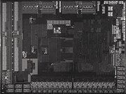
 Zen 2 I/O Die
 -
 Infrared die shot of the I/O Die
 -
 EPYC I/O Die
 -
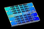 Zen 2 Core Complex Die (CCD)
 -
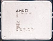 AMD EPYC 7702 server processor
 -
 AdeliddedAMD 7702 featuring 8 CCDs and 1 I/O die, with remains of the solder thermal interface material (TIM) on the chiplets


See also
[edit]References
[edit]- ^"AMD Unleashes Ultimate PC Gaming Platform with Worldwide Availability of AMD Radeon RX 5700 Series Graphics Cards and AMD Ryzen 3000 Series Desktop Processors".AMD(Press release). Santa Clara, California. 7 July 2019.Retrieved7 November2020.
- ^Larabel, Michael (16 May 2017)."AMD Talks Up Vega Frontier Edition, Epyc, Zen 2, ThreadRipper".Phoronix.Retrieved16 May2017.
- ^abCutress, Ian (20 June 2017)."AMD EPYC Launch Event Live Blog".AnandTech.Retrieved21 June2017.
- ^Boshor, Gavin (20 September 2022)."AMD Launches Mendocino APUs: Zen 2-based Ryzen and Athlon 7020 Series with RDNA 2 Graphics".AnandTech.Retrieved26 September2022.
- ^"Zen 2 - Microarchitectures - AMD".WikiChip.Retrieved14 June2020.
- ^abCutress, Ian (9 January 2019)."AMD Ryzen third Gen 'Matisse' Coming Mid 2019: Eight Core Zen 2 with PCIe 4.0 on Desktop".AnandTech.Retrieved15 January2019.
- ^online, heise (27 May 2019)."AMD Ryzen 3000: 12-Kernprozessoren für den Mainstream".c't Magazin.
- ^abLeather, Antony (7 July 2019)."AMD Ryzen 9 3900X and Ryzen 7 3700X Review: Old Ryzen Owners Look Away Now".Forbes.Retrieved13 April2023.
- ^Ridley, Jacob (27 May 2019)."AMD Ryzen 3000 CPUs launching July 7 with up to 12 cores".PCGamesN.Retrieved28 May2019.
- ^ab"2nd Gen AMD EPYC Processors Set New Standard for the Modern Datacenter with Record-Breaking Performance and Significant TCO Savings".AMD.7 August 2019.Retrieved8 August2019.
- ^Hachman, Mark (9 January 2019)."AMD's CEO Lisa Su confirms ray tracing GPU development, hints at more 3rd-gen Ryzen cores".PCWorld.Retrieved15 January2019.
- ^Curtress, Ian (26 May 2019)."AMD Ryzen 3000 Announced: Five CPUs, 12 Cores for $499, Up to 4.6 GHz, PCIe 4.0, Coming 7/7".AnandTech.Retrieved3 July2019.
- ^Thomas, Bill (10 June 2019)."AMD announces the Ryzen 9 3950X, a 16-core mainstream processor".TechRadar.Retrieved3 July2019.
- ^Alcorn, Paul (31 January 2018)."AMD Predicts Double-Digit Revenue Growth In 2018, Ramps Up GPU Production".Tom's Hardware.Retrieved31 January2018.
- ^abShilov, Anton (6 November 2018)."AMD Unveils 'Chiplet' Design Approach: 7nm Zen 2 Cores Meet 14 nm I/O Die".AnandTech.Retrieved13 April2023.
- ^Cutress, Ian (10 June 2019)."AMD Zen 2 Microarchitecture Analysis: Ryzen 3000 and EPYC Rome".AnandTech.Retrieved13 April2023.
- ^Walton, Steven (16 November 2020)."AMD Ryzen 5000 IPC Performance Tested".TechSpot.Retrieved18 April2021.
- ^Hollister, Sean (13 November 2021)."Steam Deck: Five big things we learned from Valve's developer summit".The Verge.Retrieved13 April2023.
- ^"Steam Deck:: Tech Specs".
- ^Warren, Tom (24 February 2020)."Microsoft reveals more Xbox Series X specs, confirms 12 teraflops GPU".The Verge.Retrieved24 February2020.
- ^Leadbetter, Richard (18 March 2020)."Inside PlayStation 5: the specs and the tech that deliver Sony's next-gen vision".Eurogamer.Retrieved18 March2020.
- ^abcCutress, Ian (10 June 2019)."AMD Zen 2 Microarchitecture Analysis: Ryzen 3000 and EPYC Rome".AnandTech.p. 1.Retrieved17 June2019.
- ^De Gelas, Johan (7 August 2019)."AMD Rome Second Generation EPYC Review: 2x 64-core Benchmarked".AnandTech.Retrieved29 September2019.
- ^November 2019, Paul Alcorn 21 (21 November 2019)."AMD Ryzen 9 3900X and Ryzen 7 3700X Review: Zen 2 and 7nm Unleashed".Tom's Hardware.
{{cite web}}:CS1 maint: numeric names: authors list (link) - ^Cutress, Ian (10 June 2019)."AMD Zen 2 Microarchitecture Analysis: Ryzen 3000 and EPYC Rome".AnandTech.Retrieved17 June2019.
- ^Cutress, Ian (10 June 2019)."AMD Zen 2 Microarchitecture Analysis: Ryzen 3000 and EPYC Rome".AnandTech.Retrieved17 June2019.
- ^Schor, David (22 July 2018)."VLSI 2018: GlobalFoundries 12nm Leading-Performance, 12LP".
- ^Mujtaba, Hassan (24 December 2019)."AMD Ryzen Threadripper 3970X Is An Absolutely Efficient Monster CPU".
- ^"AMD Zen 2 CPUs Come With A Few New Instructions - At Least WBNOINVD, CLWB, RDPID - Phoronix".phoronix.
- ^"GNU Binutils Adds Bits For AMD Zen 2's RDPRU + MCOMMIT Instructions - Phoronix".phoronix.
- ^btarunr (12 June 2019)."AMD Zen 2 has Hardware Mitigation for Spectre V4".TechPowerUp.Retrieved18 October2019.
- ^Agner, Fog."Surprising new feature in AMD Ryzen 3000".Agner's CPU blog.
- ^Cutress, Ian (10 June 2019)."AMD Zen 2 Microarchitecture Analysis: Ryzen 3000 and EPYC Rome".AnandTech.Retrieved12 January2023.
- ^Cutress, Ian (26 May 2019)."AMD Ryzen 3000 Announced: Five CPUs, 12 Cores for $499, Up to 4.6 GHz, PCIe 4.0, Coming 7/7".AnandTech.Retrieved17 June2019.
- ^Alcorn, Paul (14 November 2019)."Tom's Hardware Ryzen 9 3950X review".Tom's Hardware.Retrieved12 May2020.
- ^Alcorn, Paul (31 December 2020)."AMD Ryzen 9 3900X and Ryzen 7 3700X Review: Zen 2 and 7nm Unleashed".Tom's Hardware.Retrieved16 April2024.
- ^Cutress, Ian (8 October 2019)."AMD Brings Ryzen 9 3900 and Ryzen 5 3500X To Life".AnandTech.
- ^Syed, Areej (17 February 2020)."AMD Launches Ryzen 5 3500 in Japan with 6 Cores/6 Threads for 16K Yen".Hardware Times.
- ^Hill, Luke (7 February 2020)."Kitguru AMD Ryzen Threadripper 3990X CPU Review".KitGuru.Retrieved12 May2020.
- ^abLeadbetter, Richard; Judd, Will (30 July 2023)."AMD 4800S Desktop Kit review: playing PC games on the Xbox Series X CPU".Eurogamer.Retrieved20 September2023.
- ^abWhyCry (31 July 2023)."AMD 4800S Desktop Kit, a PC repurposed APU from Xbox Series X has been tested".VideoCardz.Retrieved20 September2023.
- ^abAlcorn, Paul (10 October 2021)."AMD 4700S Review: Defective PlayStation 5 Chips Resurrected".Tom's Hardware.Retrieved7 July2023.
- ^https:// techpowerup /cpu-specs/ryzen-5-4600g.c2319
- ^"AMD Spring 2022 Ryzen Desktop Processor Update Includes Six New Models Besides 5800X3D".TechPowerUp.16 March 2022.Retrieved8 March2024.
- ^"AMD Ryzen 3 PRO 4350GE".AMD.Retrieved18 October2022.
- ^"AMD Ryzen 3 PRO 4350G".AMD.Retrieved18 October2022.
- ^"AMD Ryzen 3 PRO 4650GE".AMD.Retrieved18 October2022.
- ^"AMD Ryzen 3 PRO 4650G".AMD.Retrieved18 October2022.
- ^"AMD Ryzen 3 PRO 4750GE".AMD.Retrieved18 October2022.
- ^"AMD Ryzen 3 PRO 4750G".AMD.Retrieved18 October2022.
- ^"AMD Ryzen 4000 Series Desktop Processors with AMD Radeon Graphics Set to Deliver Breakthrough Performance for Commercial and Consumer Desktop PCs".AMD.21 July 2020.Retrieved18 October2022.
- ^"AMD Ryzen 7 4800H Specs".TechPowerUp.Retrieved17 September2021.
- ^"AMD Ryzen 5 4600H Specs".TechPowerUp.Retrieved17 September2021.
- ^"AMD Ryzen 5 4600HS".AMD.[dead link]
- ^"AMD Ryzen 3 PRO 4450U".AMD.
- ^"AMD Ryzen 5 PRO 4650U".AMD.
- ^"AMD Ryzen 7 PRO 4750U".AMD.
- ^"AMD Ryzen 5 5500U Specs".TechPowerUp.Retrieved17 September2021.
- ^"AMD Details 7020 Series Ryzen and Athlon 'Mendocino' Mobile APUs".Tom's Hardware.20 September 2022.
- ^"AMD Ryzen 7020 Series Processors for Mobile Bring High-End Performance and Long Battery Life to Everyday Users".20 September 2022.Retrieved21 September2022.
- ^"AMD Ryzen 5 7520C".AMD.
- ^"AMD Ryzen 3 7320C".AMD.
- ^abcd"Product Brief: AMD Ryzen Embedded V2000 Processor Family"(PDF).AMD.
- ^"AMD Unveils AMD Ryzen Embedded V2000 Processors with Enhanced Performance and Power Efficiency".AMD.
- ^abc"New 2nd Gen AMD EPYC™ Processors Redefine Performance for Database, Commercial HPC and Hyperconverged Workloads".AMD. 14 April 2020.
- ^"AMD 4700S 8-Core Processor Desktop Kit".AMD.Retrieved26 September2022.